What are fluids?
A fluid is a substance that can flow. The fluid has no definite shape. Its shapes depends upon the containing vessel i.e. It cannot resist shearing stress and adjust their form accordingly.
What is ideal fluid?
Those fluid which have zero compressibility and zero viscosity is called ideal fluid.
Important characteristics of fluids :
(1) Random Molecular Arrangment: The atoms or molecules within a fluid are arranged randomly unlike the structured arrangment in a solid.
(2) Inability to resist shearing stress: A fluid cannot withstand tangential or shearing stress for an indefinite period. When a shearing stress is applied, it begins to flow.
(3) No fixed shape: A fluid has no definite shape of its own and it adopt the shape of their container. Consequently, a fluid does not possess modulus of rigidity.
(4) Ability to exert perpendicular force: A fluid exert a force in a direction normal to its surface. Consequently, a fluid does possess bulk modulus of rigidity.
Basics of Semiconductor Materials
Semiconductor materials:
Those materials with conductivity greater than insulators and less than conductors are known as semiconductor materials.
According to band gap theory:
Those materials that have a band gap between the conduction band and the valence band is approximately one electron volt are called semiconductor materials.
Description of semiconductor material based on Bandgap theory:
a.) At Room temperature:
The conduction band and valence band are partially filled at room temperature.

b.) At very high temperature:
At very high temperatures, the conduction band is completely filled and the valence completely empty due to this, the semiconductor behaves like a conductor.

c.) At very low temperature:
At very low temperatures, the conduction band is completely empty and the valence band is completely filled due to this the semiconductor behaves like an insulator.

Types of semiconductor material:
There are two types of semiconductor materials:
1.) Intrinsic semiconductor materials
2.) Extrinsic semiconductor materials
1.) Intrinsic semiconductor materials:
The pure form of the semiconductor materials is known as intrinsic semiconductor materials.
Examples: Carbon, Germanium, Silicon, etc.
General description:
Intrinsic semiconductor material is the pure form of the semiconductor material like carbon Germanium silicon. The atoms of the semiconductor material has four valence electrons and tightly bound to the nucleus. all the atoms are bound with covalent bonds.
 At very low temperatures or Absolute temperatures, all valence electrons are tightly bound to the core of the atom and no free electrons are available to conduct electricity through the semiconductor crystal.
At room temperature, a few valence electrons are thermally excited into the conduction band and free to move about. These few thermally excited electrons leave holes in the valence band. the conductivity of an intrinsic semiconductor is very poor that is only one covalent bond breaks in $10^{9}$ atoms of a semiconductor like Germanium. It means that only one atom in $10^{9}$ atoms is available for conduction. The concentration of free electrons and holes in intrinsic semiconductors are equal.
At very high temperatures, a large number of electrons and holes are produced. When an electric field is applied to the semiconductor crystal the free electrons in the conduction band move in the opposite direction of the applied field and holes in the valence band move in the direction of the applied field, both give rise to electric current. The motion of holes is apparent.

2.) Extrinsic semiconductor materials:
When a small amount of impurity (i.e. external material atoms) is added to intrinsic semiconductor materials then these materials are known as extrinsic semiconductor materials.
Note:
a.) What is doping?
Answer: The process of adding a small amount of impurity atoms in intrinsic semiconductor materials is known as doping.
b.) What is impurity or doped semiconductor?
Answer: The impurity or doped semiconductor is the atoms of external material with a valency of pentavalent or trivalent.
The pentavalent impurity atom (i.e. outer shell has $+5$ electrons) is also called the donor atom. Because it donates conducting electrons to the atom of a semiconductor crystal. The trivalent impurity atom (i.e. outer shell has $+3$ electrons) is also called the acceptor atom. Because it accepts the conducting electron from the neighbor atom of the semiconductor crystal.
Example: $1$ impurity atom added in $108$ semiconductors atoms of Germanium increases the conductivity of $16$ times
Example:
Pentavalent: Antimony, Phosphorus or arsenic etc.
Trivalent: Boron, Aluminium, Gallium or Indium etc
Types of extrinsic semiconductor materials:
The extrinsic semiconductor materials are two types-
i.) N-Type Semiconductor Materials
ii.) P-Type Semiconductor Materials
i.) N-Type Semiconductor Materials:
General description:
 When the pentavalent impurity atoms (like Phosphorus) are added to the semiconductor materials (like $Ge$), they replace the semiconductor atoms and take place in between them. Now the four electrons of the pentavalent atom make the covalent bond with neighbor semiconductor atoms. Still, the fifth electron does not make the covalent bond. It becomes free (a very small amount of energy is required to free i.e. $0.01 eV $ in $Ge$ and $0.05 eV $ for $Si$ lattice) at room temperature and moves in semiconductor crystal as charge-carrier. The electrons are charge carriers because of that it is called negative-type semiconductors or n-type semiconductors.
ii.) P- Type Semiconductor Materials:
When a very small amount of trivalent impurity atoms are added to the intrinsic semiconductor material, this semiconductor material is known as a p-type semiconductor. The holes in p-type semiconductors are majority charge carriers.
General description:
 When the trivalent impurity atoms (like Boron) are added to the semiconductor materials (like $Ge$), it replace the semiconductor atoms and take place them. Now the three electrons of the pentavalent atom make the covalent bond with neighbor semiconductor atoms but the fourth electron of the neighbor semiconductor atom does not make the covalent bond with the trivalent impurity atom because of that and empty space is created near the trivalent atom. This empty space is called a hole. A hole moves in the semiconductor crystal as a charge carrier in the opposite direction of the flow of electrons (or in the direction of an external electric field) in the presence of an external electric field. These charge-carries act as positive charge-carries because of that it is called positive-type semiconductors or p-type semiconductors.
Note:
Explanation of flow of hole in semiconductor crystal:
When an external field is applied, an electron of a semiconductor atom bound near a trivalent impurity atom moves toward a hole (near to impurity atom) and leaves the new hole behind. This process is continuous and the hole moves in the semiconductor crystal in the direction of an external electric field or in the opposite direction of electron flow ( i.e. aThe electric potential of electron is negative and the hole is zero so electron move from lower potential to higher potential.).


2.) Extrinsic semiconductor materials


Pentavalent: Antimony, Phosphorus or arsenic etc.
Trivalent: Boron, Aluminium, Gallium or Indium etc
ii.) P-Type Semiconductor Materials
When a very small amount of pentavalent impurity atoms are added to the intrinsic semiconductor material, this semiconductor material is known as an n-type semiconductor. The electrons in n-type semiconductors are majority charge carriers.


Binding Energy Curve
Binding Energy Curve :
 There are following discussion point obtained from the binding energy curve :
1.) For Nuclei with $A=50$ TO $A=80$:
For nuclei with atomic mass number $A = 50 - 80$ , the B.E./ nucleon (i.e. binding energy per nucleon) is approximately $8.5 MeV$.
The curve is almost flat in this and indicate the highly stability of the nucleus.
2.) For Nuclei with $A \geq 80$:
For heavier nuclei with $A \gt 80$, the B.E. /nucleon ( i.e. binding energy per nucleon) decreases slowly and reaching about $7.6 MeV$ for uranium ($U \: A = 238$).
The lower value of binding energy per nucleon fails to counteract the Coulombian repulsion among protons in nuclei having large number of protons resulting instability
Consequently, the nuclei of heavier atoms beyond $_{83}Bi^{209}$ are radioactive.
3.) For Nuclei with $A \leq 50$:
For nuclei with atomic mass number below $50$ , the B.E./ nucleon decreases, with a sharp drop below $A=20$.
For example: Heavy hydrogen (i.e $_{1}H^{2}$), it is only about $1.1 MeV$. it indicates that lower stability for nuclear with mass number below $20$.
4.) Subsidiary Peak for $A \lt 50$:
Below $A = 50$, the curve does not fall continuously, but the subsidiary peaks at $_{8}O^{16}, _{6}C^{12},_{2}He^{4}$.
These peak indicate that such even-even nuclear are more stable compared to the immediate neighbours .
5.) Nuclear fusion and Nuclear fission process release energy:
From curve, it shows that drops down in curve at both high and low mass number and lower binding energy per nucleon.
For example:
A very high amount of energy is released in the process of nuclear fission and fusion because of Lo binding energy causes instability of the nucleus.
A graph is plotted for different nuclei between the binding energy per nucleon and the atomic mass number. This graph gives a curve which is called " binding energy curve".

Nuclear Fission and Nuclear Fusion
Nuclear Fission:
Example:
$_{92}U^{235} +\: _{0}n^{1} (Neutron) \rightarrow \: _{92}U^{236} \rightarrow _{56}Ba^{141} + \: _{36}Kr^{92} + \: 3 _{0}n^{1} + \gamma$
Nuclear Fusion:
Example: Two deuterons can be fused to form a triton(tritium nucleus) as shown in the reaction below:
$_{1}H^{2} + \: _{1}H^{2} \rightarrow \: _{1}H^{3} + \: _{1}H^{1} + \: 4.0 \: MeV \:(Energy)$
$_{1}H^{3} (Tritium) + _{1}H^{2} \rightarrow \: _{2}He^{4} + _{0}n^{1} + 17.6.0 \: MeV \:(Energy)$
The total result of the above two equations is the fusion of deuterons and produces an $\alpha - $ particle $(_{2}He^{4})$, a neutron $(_{0}n^{1})$ and a proton $(_{1}H^{1})$. The total released energy is $21.6 MeV$.
Alternatively, the fusion of three deutrons $(_{1}H^{2})$ into $\alpha -$ partice can takes place as follows:
$_{1}H^{2} + _{1}H^{2} \rightarrow \: _{2}He^{3} + _{0}n^{1} + 3.3 \: MeV \:(Energy)$
$_{2}He^{3} + _{1}H^{2} \rightarrow \: _{2}He^{4} + _{1}H^{1} + 18.3 \: MeV \:(Energy)$
When a heavy nucleus breaks into two or more smaller, lighter nuclei and produces high energy, this process is called as nuclear fission.
When two or more very light nuclei move with a very high speed then these nuclei are fused and form a single nucleus. This process is called as nuclear fusion.
Mass Defect, Binding Energy and Binding Energy per nucleon
Binding Energy:
Where
$\Delta m \rightarrow$ Mass Defect
$P \rightarrow$ Number of Proton
$N \rightarrow$ Number of Neutron
$m_{actual} \rightarrow$ Actual mass of nucleus
$m_{P} \rightarrow$ Mass of a Proton
$m_{N} \rightarrow$ Mass of a Neutron
We know that
$Z=P=e \\ N=A-Z \qquad (2)$
Where
$Z \rightarrow $ Atomic Number
$A \rightarrow $ Atomic Mass Number
$ e \rightarrow $ Number of Electrons
From above two equation $(1)$ and equation $(2)$
$\Delta m = \left [ Z \times m_{P} + \left ( A-Z \right) \times m_{N} \right] - m_{actual} \qquad (1)$
Binding Energy:
Where $B.E.\rightarrow$ Binding Energy
$B.E= \Delta m (in \: a.m.u.) \times 931.5 \: MeV$
Where $1 \: a.m.u. = 1.67377 \times 10^{-27} kilograms$
Binding energy per nucleon:
Where $B.E.\rightarrow$ Binding Energy
Note: Higher binding energy per nucleon shows higher stability of the nucleus.
The difference between the total mass of individual nucleons (i.e. total number of proton and neutron) and actual mass of nucleus of that energy is called binding energy.$\Delta m = \left (P \times m_{P} + N \times m_{N} \right) - m_{actual} \qquad (1)$
$\Delta m \rightarrow$ Mass Defect
$P \rightarrow$ Number of Proton
$N \rightarrow$ Number of Neutron
$m_{actual} \rightarrow$ Actual mass of nucleus
$m_{P} \rightarrow$ Mass of a Proton
$m_{N} \rightarrow$ Mass of a Neutron
$Z \rightarrow $ Atomic Number
$A \rightarrow $ Atomic Mass Number
$ e \rightarrow $ Number of Electrons
The energy require to form or break a nucleous is called the binding energy of nucleous.$B.E= \Delta m \times c^{2} Joule$
The energy require to emit one nucleon from the nucleous is called binding energy per nucleon.$B.E. \: per \: nucleon = \frac{B.E.}{ Total \: No. \: of \: Nucleons}$
Spectrum of Hydrogen Atom
Description:
The different series of hydrogen spectra can be explained by Bohr's theory. According to Bohr's theory, If the ionized state of a hydrogen atom be taken zero energy level, then energies of different energy levels of the atom can be expressed by following the formula
$E_{n}=\frac{Rhc}{n^{2}} \qquad (1)$
Where
$R \rightarrow$ Rydberg's Constant
$h \rightarrow$ Planck's Constant
$n \rightarrow$ Quantum Number
According to Plank's Theory
$E_{2} - E_{1} =h \nu \qquad(2)$
So from equation $(1)$
$E_{1}=\frac{Rhc}{n^{2}_{1}} $ and $E_{2}=\frac{Rhc}{n^{2}_{2}} \qquad (3)$
From equation $(2)$ and equation $(3)$
$\frac{Rhc}{n^{2}_{2}} - \frac{Rhc}{n^{2}_{1}} =h \nu $
$\frac{Rhc}{n^{2}_{2}} - \frac{Rhc}{n^{2}_{1}} = \frac{hc}{\lambda} $
$\frac{1}{\lambda}=R \left(\frac{1}{n^{2}_{1}} -\frac{1}{n^{2}_{2}} \right)$
The quantity $\frac{1}{\lambda}$ is called the 'wave number', All the series found in the hydrogen spectrum are explained by the above
equation :
 (i) Lyman Series: When an atom comes down from some higher energy level (i.e. $n_{2} = 2, 3, 4, ...$) to the first energy level (lowest energy level), (i.e. $n_{1}= 1$), then spectral lines are emitted in the spectrum region of ultraviolet. The equation for obtaining the wavelengths of these spectral lines:
$\frac{1}{\lambda}=R \left(\frac{1}{1^{2}} -\frac{1}{n^{2}_{2}} \right)$
Where $n_{2} = 2, 3, 4, ...$
In 1916, Lyman photographed the lines of this series of hydrogen spectra. Hence, this series is named Lyman series'. The longest wavelength of this series (for $n_{2} = 2$) is $1216 A^{\circ}$ and the shortest wavelength (for $n_{2} = \infty$) is $912 A^{\circ}$. The wavelength $912 A^{\circ}$ corresponding to $n = \infty$ is called the 'series limit'.
(ii) Balmer Series: When an atom comes down from some higher energy level (i.e. $n_{2} = 3, 4, 5, ...$) to the second energy level (i.e. $n_{1}= 2$), then the spectral lines are emitted in the spectrum region of the visible part.
$\frac{1}{\lambda}=R \left(\frac{1}{2^{2}} -\frac{1}{n^{2}_{2}} \right)$
where $n_{2} = 3, 4, 5, ...$
In 1885, Balmer saw and studied first time these spectral lines. The longest wavelength of this series (for $n_{2} = 3$) is $6563 Å$ and the shortest wavelength (for $n_{2} = \infty$) is 3646 Ä.
(iii) Paschen Series: When an atom comes down from some higher energy level (i.e. $n_{2} = 3, 4, 5, ...$) to the third energy level (i.e. $n_{1}= 3$) then the spectral lines are emitted in the spectrum region of infrared.
$\frac{1}{\lambda}=R \left(\frac{1}{3^{2}} -\frac{1}{n^{2}_{2}} \right)$
where $n_{2} = 4, 5, 6, ...$
(iv) Brackett Series: When an atom comes down from some higher energy level (i.e. $n_{2} = 5, 6, 7, ...$) to the fourth energy level (i.e. $n_{1}= 4$), then the spectral lines are also emitted in the spectrum region of infrared.
$\frac{1}{\lambda}=R \left(\frac{1}{4^{2}} -\frac{1}{n^{2}_{2}} \right)$
where $n_{2} = 5,6, 7,.....$
(iv) Pfund Series: When an atom comes down from some higher energy level (i.e. $n_{2} = 6, 7, 8, ...$) to the fifth energy level (i.e. $n_{1}= 5$) then the spectral lines are also emitted in the spectrum region of infrared.
$\frac{1}{\lambda}=R \left(\frac{1}{5^{2}} -\frac{1}{n^{2}_{2}} \right)$
where $n_{2}= 6,7, 8, ....$
$R \rightarrow$ Rydberg's Constant
$h \rightarrow$ Planck's Constant
$n \rightarrow$ Quantum Number

Radioactive Decay and its types
Definition:
There are 3- types of radioactive decay
1. Alpha Decay
2. Beta Decay
3. Gamma Decay
1. Alpha Decay: A helium nuclei which contain two protons and two neutrons is known as an alpha particle. The $\alpha$- particles are commonly emitted by the heavier radioactive nuclei. When the $\alpha$- particle is emitted from the nucleus then the atomic number is reduced by two (i.e. $Z-2$) or the atomic mass number is reduced by 4 (i.e. $A-4$).
Example:
The decay of $Pu^{239}$ into fissionable $U^{235}$ by the emission of $alpha$- particle
$_{94}Pu^{214} \rightarrow _{92}U^{235} + _{2}He^{4} \left(\alpha - particle \right)$
2. Beta Decay: The emission of $\beta$-particle occurs due to the conversion of a neutron into a proton or vice versa in the nucleus. The $\beta$-decay is commonly accompanied by the emission of neutrino ($\nu$) radiation. There are two types of $\beta$-decay.
i.) Beta Minus: When a neutron is converted into a proton then an electron ($_{-1}e^{\circ}$) i.e.$\beta$-minus particle is emitted. When the $\beta$- minus particle is emitted from the nucleus then the atomic number is increased by one (i.e. $Z+1$) and no change in atomic mass number ($A$).
Example:
$_{6}C^{14} \rightarrow _{7}N^{14} + _{-1}e^{\circ} + \overline{\nu}_{e} \: (anti\:neutrino)$
ii.) Beta Plus: When a proton is converted into a neutron then a positron ($_{+1}e^{\circ}$) $\beta$- plus partice is emitted. When the $\beta$- plus particle is emitted from the nucleus then the atomic number is decreased by one (i.e. $Z-1$) and no change in atomic mass number ($A$). It is also known as positron decay. Positron decay is caused when the radioactive nucleus contains an excess of protons.
Example:
$_{12}Mg^{23} \rightarrow _{11}Na^{23} + _{+1}e^{\circ} + \nu_{e}\: (neutrino)$
The penetrating power of $_{-1}\beta^{\circ}$ particles is small compared to $\gamma$-rays, however it is larger than that of $\alpha$-particles.
Note:
Electron Capture: The nucleus captures the electron from orbits and combines with a proton to form a neutron and emits a neutrino.
Example:
$_{26}Fe^{55} + _{-1}e^{\circ} \rightarrow _{25}Mn^{55} + \nu_{e}\: (neutrino)$
3. Gamma (y) Decay: $\gamma$-particles are electromagnetic radiation of extremely short wavelength and high frequency resulting in high energy. The $\gamma$-rays originate from the nucleus while X-rays come from the atom. $\gamma$-wavelength are on average, about one-tenth those of X-rays, though energy ranges overlap somewhat. There is no alternation of atomic or mass numbers due to $\gamma$ decay.
Example:
$_{27}Co^{60} \rightarrow _{27}Co^{60} + \gamma \: (gamma)$
When the unstable atom (called radionuclide) loses its energy through ionizing radiation, this process is known as radioactive decay.Types of radioactive decay:
2. Beta Decay
3. Gamma Decay
Combination of cell in the circuit
A.) Combination of cells when emf of cells are same:
There are three types of combinations of cells in the circuit
1.) Series Combination of Cells
2.) Parallel Combination of Cells
3.) Mixed Combination of Cells
1.) Series Combination of Cells: Let us consider that the $n$ - cells having emf (electromotive force) $E$ and internal resistance $r$ are connected in series with external resistance $R$. Then from the figure given below
 The total emf of the $n$ - cell = $nE$
The total internal resistance of the $n$ - cell = $nr$
The total resistance of the circuit = $nr+R$
The total current in the circuit
$i=\frac{Total \: emf \: of \: the \: n - series \: cell}{Total \: resistance \: of \: the \: circuit}$
$i=\frac{nE}{nr+R}$
2.) Parallel Combination of Cells: Let us consider that the $n$ - cells having emf (electromotive force) $E$ and internal resistance $r$ are connected in parallel with external resistance $R$. Then from the figure given below
 The total emf of the $n$ - cell = $E$
The total internal resistance of the $n$ - cell
$\frac{1}{r_{eq}} = \frac{1}{r}+ \frac{1}{r}+.........n \: times$
$\frac{1}{r_{eq}}=\frac{n}{r}$
$r_{eq}=\frac{r}{n}$
The total resistance of the circuit = $\frac{r}{n}+R$
The total current in the circuit
$i=\frac{Total \: emf \: of \: the \: n - parallel \: cell}{Total \: resistance \: of \: the \: circuit}$
$i=\frac{E}{\frac{r}{n}+R}$
$i=\frac{E}{\frac{r+nR}{n}}$
$i=\frac{nE}{r+nR}$
3.) Mixed Combination of Cells: Let us consider that the $n$ - cells having emf (electromotive force) $E$ and internal resistance $r$ are connected in series in each row of $m$ parallel rows with external resistance $R$. Then from the figure given below
 The total emf of the $n$ - cell in each row of $m$ parallel rows of the cells = $nE$
The internal resistance of the $n$ - cell in each row = $nr$
The total internal resistance of the $n$ - cell in each of $m$ parallel rows of the cells = $nr$
$\frac{1}{r_{eq}} = \frac{1}{nr}+ \frac{1}{nr}+.........m \: times$
$\frac{1}{r_{eq}}=\frac{m}{nr}$
$r_{eq}=\frac{nr}{m}$
The total resistance of the circuit = $\frac{nr}{m}+R$
The total current in the circuit
$i=\frac{Total \: emf \: of \: the \: cell}{Total \: resistance \: of \: the \: circuit}$
$i=\frac{nE}{\frac{nr}{m}+R}$
$i=\frac{nE}{\frac{nr+mR}{m}}$
$i=\frac{mnE}{nr+mR}$
It is clear from the above equation that for the value of $i$ to be maximum, the value of $(nr+mR)$ should be minimum. Now,
$nr+mR= \left[ \sqrt{nr}-\sqrt{mr} \right]^{2}+2 \sqrt{mnRr}$
Therefore, for $(nr+mR)$ to be minimum, the quantity $\left[ \sqrt{nr}-\sqrt{mr} \right]^{2}$ should be minimum. So
$\left[ \sqrt{nr}-\sqrt{mr} \right]^{2} = 0$
$ \sqrt{nr}-\sqrt{mr} = 0$
$ \sqrt{nr} = \sqrt{mr} $
$nr=mR$
$R=\frac{nr}{m}$
Here, $\frac{nr}{m}$ is the total resistance of the cells.
Thus, When the total internal resistance of the cells are equal to the external resistance then the total current in the external circuit will be maximum in the mixed combination of cells.


Relation between electromotive force (E), internal resistance (r) and potential difference (V) in a circuit
Relation between electromotive force $(E)$, internal resistance $(r)$ and potential difference $(V)$:
Let us consider:
The cell having electro-motive force = $E$
The cell having internal resistance = $r$
The external resistance of the circuit = $R$
The potential difference between the external resistance of the circuit = $V$
The current in circuit = $i$
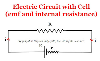.jpg "Electric Circuit with Cell (emf and internal resistance)") So, The emf of the cell from the given circuit in the figure above
So, The emf of the cell from the given circuit in the figure above
$E=iR+ir$
$E = V+ir$
$V=E-ir$
")
Resolving Power of Optical Instrument | Rayleigh Criterion of Resolution
Resolving power of an optical instrument:
The ability of an optical instrument to just resolve the images of two closely spaced objects is called its resolving power.
Limit of Resolution:
The smallest distance between two closely spaced objects that can be seen as separated or just separated from each other through an optical instrument is known as the limit of resolution of that optical instrument.
Rayleigh Criterion:
Rayleigh criterion describes the separation between the two objects or wavelengths (i.e. resolving power) by the resultant intensity distribution of objects and wavelengths. According to Rayleigh's criterion, there are the following cases:
Case:1 If two point sources have very small angular separation, then central or principal maxima in their diffraction patterns will overlap to a large extent and resultant intensity shows uniform variation. As shown in the figure below. In this case, the two objects or wavelengths can not be distinguished or unresolved.

Case:2 If two point sources have very large angular separation then the central or principal maxima are widely separated and the resultant intensity shows two widely separated peaks. As shown in the figure below. In this case, the objects or wavelengths are resolved well.

Case:3 If the central or principal maxima in the diffraction pattern of one object or wavelength coincide with the first minima in the diffraction pattern of the other objects or wavelength then the resultant intensity shows a small dip. As shown in the figure below. In this case, the objects or wavelengths are seen to be just separate or just resolved.


Attenuation of optical signal in optical fibre
Attenuation (or Loss) of optical signal in optical Fibre:
The difference in the power of the input optical signals and output optical output signals in optical fibre is known as attenuation in the optical fibre. It is measured in decibels per kilometer $(\frac{dB}{Km})$ and caused by the absorption and scattering of the optical signal in optical fibre.
The optical signal strength is reduced when the signal travels in optical fibre over a long distance. The expression for the attenuation of optical signal in optical fibre:
$\alpha = - \frac{10}{x(Km)} log \left[ \frac{P_{x}}{P_{\circ}} \right]$
Where
$P_{x} \rightarrow $ Power of optical signal at a position $x$ from origin
$P_{\circ} \rightarrow $ Power of optical signal at origin
The Losses in optical fibre are wavelength-dependent and the attenuation factor depends on the fibre material and manufacturing tolerance.
Types of Attenuation or Loss
A.) Absorption Attenuation or Loss
B.) Scattering Attenuation or Loss
C.) Bending Attenuation or Loss
A.) Absorption Attenuation or Loss:
The absorption of optical signals in optical fibre depends on the amount of the material in optical fibre. There are two types of absorption on optical fibre:
1.) Intrinsic Material Absorption
2.) Extrinsic Material Absorption
1.) Intrinsic Material Absorption: It is a fundamental minimum loss due to absorption when the optical signal passes through the optical fibre. This absorption occurs due to material in optical fibre with no impurities.
2.) Extrinsic Material Absorption: It is a loss due to absorption when the optical signal passes through the optical fibre. This absorption occurs due to a material having impurities ( such as $Fe^{+2}, Cu^{+2}, Cr^{+3}, and \: OH^{-}$ ion from water dissolved in glass) in the optical fibre material.
B.) Scattering Attenuation or Loss:
When the optical signal interacts with a particle then the energy of the optical signal is reduced and it goes in another direction. In scattering, the optical signal is not absorbed but it goes to any other direction which also causes the loss of the optical signal. Scattering is the loss of optical signal due to imperfections in the optical fibre i.e. the basic structure of the optical fibre. There are two types of scattering that occur in the optical fibre i.e.
1.) Linear Scattering:
2.) Nonlinear Scattering
1.) Linear Scattering: The amount of power of the optical signal transferred from an optical wave is proportional to power. There is no change in the frequency of the optical signal.
Types of Linear Scattering
i.) Rayleigh scattering in optical fibre
ii.) Mie scattering in optical fibre
i.) Rayleigh scattering in optical fibre: When the optical signal interacts with the lattice of the core it causes the scattering because the size of the lattice is smaller than the wavelength of the incident optical signal. This interaction is also known as elastic scattering.
In optical fibres, This scattering controls the intrinsic loss mechanism in the low-absorption between absorption tails of the ultraviolet and infrared. This is caused by random heterogeneity in the material of the core lattice that leads to changes in the refractive index. These changes cause attenuation in the optical signal by scattering in optical fibre.
ii.) Mie scattering in optical fibre: When the optical signal interacts with the lattice of the core that causes the scattering because in this scattering the size of a lattice is comparable to the wavelength of the incident optical signal. This interaction is also known as elastic scattering.
In optical fibres, This scattering occurs when the optical signal interacts with inhomogeneities in the fibre core or cladding that are larger than the wavelength of the incident optical signal.
2.) Nonlinear scattering: It is an inelastic scattering that occurs when an optical signal interacts with a material in a non-linear manner. Non-linear scattering occurs, when the intensity of the incident optical signal is very high to change the refractive index of material or when the optical signal interacts with molecules or particles that have non-linear optical properties.
In non-linear scattering, the intensity of the scattered optical signal is not proportional to the intensity of the incident optical signal, and the scattered optical signal can be polarized in different planes than the incident optical signal.
In other words,
In non-linear scattering the wavelength, frequency, or phase of scattered optical signal is different than the incident optical signal. The energy and momentum of the scattered optical signal are not conserved, hence, the scattered optical signal has different characteristics than the incident optical signal.
Types of Non-linear Scattering:
i.) Raman Scattering
ii.) Brillouin Scattering
iii.) Self-phase modulation (SPM)
iv.) Cross-phase modulation (XPM)
v.) Four-wave mixing (FWM)
i.) Raman Scattering: It is an inelastic scattering that occurs when a photon of optical signal interacts with molecules of vibrational modes in the material of the core then this photon excites the molecule to a virtual state before being re-emitted in a different direction with a different energy and frequency.
The frequency shift of the scattered optical signal is directly related to the molecule's vibrational energy, which is a characteristic property of the material.
Stimulated Raman scattering $(SRS)$ is an optical process (i.e. nonlinear process ) that enhances scattering by stimulating the molecules of vibrational modes. In SRS, a pump beam of high intensity is used to amplify the Raman signal which leads to a strong and more easily detectable output optical signal.
ii.) Brillouin Scattering: It is an inelastic scattering that occurs when an optical signal interacts with a material, usually a solid or a liquid, causing the material to vibrate.
It can also be said to be a scattering that occurs due to the interaction of an incident optical signal with the acoustic wave in a material.
The vibrating material scatters the optical signal, shifting its frequency by an amount proportional to the frequency of the vibration.
The scattering of the light by the vibrating material is called the Brillouin scattering. This scattering can be either stimulated or spontaneous. It depends on the material that is excited by an external stimulus or its own oscillations.
Stimulated Brillouin scattering (SBS) is used to control the optical signals in optical fibers and other waveguides. When the frequency of the incident optical signal is tuned to the frequency of the vibrational modes of the fiber then the scattered optical signal is shifted to a new frequency which allows for attenuation or amplification of the optical signal.
Brillouin scattering has various applications in materials science. It is used to study the mechanical properties of materials and to determine the stress and strain in solid materials.
iii.) Self-phase modulation (SPM): It is a non-linear effect that occurs when the optical signal of high intensity travels through an optical fiber. The intensity of the optical signal causes a change in the refractive index of the optical fiber that causes a phase shift in the optical signal.
This phase shift can cause the optical signal to spread out in time and frequency which leads to distortion of the transmitted signal.
In other words, The optical signal pulses change their spectrum due to their own intensity from an induced varying refractive index of the medium.
iv.) Cross-phase modulation (XPM): It is a non-linear effect that occurs when two optical signals, typically from two different channels, interact with each other in an optical fiber.
The interaction between the optical signals causes a change in the refractive index of the fiber, that causes a phase shift in one of the optical signals.
This phase shift can distort the optical signal which can lead to crosstalk between different channels in a fiber optic communication system.
v.) Four-wave mixing (FWM): It is a non-linear effect that occurs when two or more incident optical signals interact with each other in a non-linear medium and produce a new wave with a different frequency and phase.
It is used for wavelength conversion of optical signals and signal processing in optical fibers.
C.) Bending Attenuation or Loss: It is caused by the bending of optical fibre or physical stress on the fibre.
Types of Bend Loss
a.) Microbend Loss
b.) Macrobend Loss
a.) Microbend Loss: It is caused by small discountinuities or imperfections in the optical fibre. Microbend loss increses due uneven coating applications and improper cabling procedures. The external force is also a source of micro bending.
b.) Macrobend Loss: It is caused when the fibre bend's radius of curvature is larger than the fibre diametre. These bends are a great source of loss when the radius of curvature is less than several centimetres.
$P_{x} \rightarrow $ Power of optical signal at a position $x$ from origin
$P_{\circ} \rightarrow $ Power of optical signal at origin
B.) Scattering Attenuation or Loss
C.) Bending Attenuation or Loss
2.) Extrinsic Material Absorption
2.) Nonlinear Scattering
ii.) Mie scattering in optical fibre
ii.) Brillouin Scattering
iii.) Self-phase modulation (SPM)
iv.) Cross-phase modulation (XPM)
v.) Four-wave mixing (FWM)
b.) Macrobend Loss
Popular Posts
-
 Angle of Acceptance → "If incident angle of light on the core for which the incident angle on the core-cladding interface equals t...
 -
Let $S$ be a point monochromatic source of light of wavelength $\lambda$ placed at the focus of collimating lens $L_{1}$. The light beam is ...
-
Maxwell's Equations: Maxwell's equation of the electromagnetic wave is a collection of four equations i.e. Gauss's law of elec...
-
Derivation of interference of light due to a wedge-shaped thin film: Interference of light due to wedge-shaped thin film The wedge...
-
Let a plane wavefront be incident normally on slit $S_{1}$ and $S_{2}$ of equal $e$ and separated by an opaque distance $d$.The diffracted l...


