Paramagnetic Substances :
Those substances, which are placed in the external magnetic field and they are weakly magnetized in the direction of the external magnetic field, are called paramagnetic substances.
The susceptibility $\chi_{m} $ of paramagnetic substances is small and positive. Further, When a paramagnetic substance is placed in the magnetic field, then the flux density of the paramagnetic substance is slightly more than the free space. Thus, the relative permeability of paramagnetic substance $\mu_{r}$, is slightly more than 1.
Properties of Paramagnetic substances:
1. When a rod of a paramagnetic material is suspended freely between external magnetic poles (i.e. Between North and South Poles) then its axis becomes along the direction of the external magnetic field $B$ (Figure). The poles produced on the two sides of the rod are opposite to the poles of the external magnetic field.
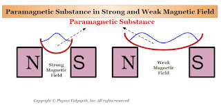
2. In a non-uniform magnetic field, a paramagnetic substance tends to move from the weaker magnetic field to the stronger magnetic field. If a paramagnetic liquid is taken in a watch glass placed on two magnetic poles very near to each other, then the liquid rises in the middle as shown in the figure below(Figure) where the field is strongest. Now, if the distance between the poles is increased, the liquid is depressed in the middle, because now the field is strongest near the poles.
3. If the solution of a paramagnetic substance is poured into a U-tube and apply the strong magnetic field into one arm of this U-tube then the level of the solution in that arm rises. As shown in the figure below:
4. When paramagnetic gas molecules are passed between the poles of a magnet then paramagnetic gas molecules are attracted toward the magnetic field.
5. The susceptibility of a paramagnetic substance is inversely dependent on temperature.
$\chi \propto \frac{1}{T_{C}-T}$
Explanation of Paramagnetism on the Basis of Atomic Model:
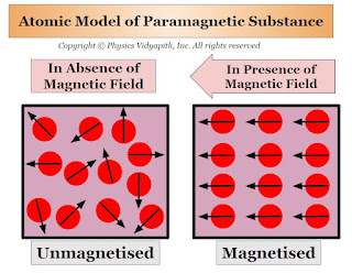
The property of Paramagnetism is generally found in those substances whose atoms (or ions or molecules) have an 'odd' number of electrons. In these odd numbers of electrons one electron is not able to form a pair because the net magnetic dipole moment of the atoms (or ions or molecules) are not zero. but in the absence of an external magnetic field, these magnetic dipole moments are randomly arranged inside the substance because the net magnetic dipole moment of the material is zero.
When a paramagnetic substance is placed in an external magnetic field $B$ then the magnetic dipole moment of the atoms (or ions or molecules) are weakly aligned in the direction of the external magnetic field. Thus, a small magnetic dipole moment is induced in the substance which is directly proportional to the magnetic field $B$. Hence, the paramagnetic substance is magnetized in the direction of the external magnetic field $B$, and the field lines become less dense inside the paramagnetic substance compared to those outside.
Work energy theorem Statement and Derivation
Work-energy theorem statement:
The work between the two positions is always equal to the change in kinetic energy between these positions. This is known as the work energy Theorem.
$W=K_{f}-K_{i}$
$W=\Delta K$
Derivation of the Work-energy theorem:
According to the equation of motion:
$v^{2}_{B}=v^{2}_{A}+2as $
$2as=v^{2}_{B}-v^{2}_{A}$
$2mas=m(v^{2}_{B}-v^{2}_{A})$
$mas=\frac{m}{2} (v^{2}_{B}-v^{2}_{A})$
$Fs=\frac{1}{2}mv^{2}_{B}-\frac{1}{2}mv^{2}_{A} \qquad (\because F=ma)$
$W=\frac{1}{2}mv^{2}_{B}-\frac{1}{2}mv^{2}_{A} \qquad (\because W=Fs)$
$W=K_{f}-K_{i}$
Where
$K_{f}$= Final Kinetic Energy at position $B$
$K_{i}$= Initial Kinetic Energy at position $A$
$W=\Delta K$
Alternative Method (Integration Method):
We know that the work done by force on a particle from position $A$ to position $B$ is-
$W=\int F ds$
$W=\int (ma)ds \qquad (\because F=ma)$
$W=m \int \frac{dv}{dt}ds$
$W=m \int dv \frac{ds}{dt}$
$W=m \int v dv \qquad (\because v=\frac{ds}{dt})$
If position $A$ is the initial point where velocity is $v_{A}$ and position $B$ is the final point where velocity is $v_{B}$ then work is done by force under the limit-
$W=m \int_{v_{A}}^{v_{B}} v dv$
$W=m[\frac{v^{2}}{2}]_{v_{A}}^{v_{B}} $
$W=\frac{1}{2}mv^{2}_{B}-\frac{1}{2}mv^{2}_{A}$
$W=K_{f}-K_{i}$
$W=\Delta {K}$
$K_{f}$= Final Kinetic Energy at position $B$
$K_{i}$= Initial Kinetic Energy at position $A$
Davisson and Germer's Experiment and Verification of the de-Broglie Relation
Davisson and Germer's Experiment on Electron Diffraction:
Davisson and Germer's experiment verifies the wave nature of electrons with the help of diffraction of the electron beam as wave nature exhibits the diffraction phenomenon.
Principle: The principle of Davisson and Germer's experiment is based on the diffraction phenomenon of the electron beam by crystal and it verifies the de-Broglie relation.
Theoretical Formula: If a narrow beam of electrons is accelerated by a potential difference $V$ volts, the kinetic energy $K$ acquired by each electron in the beam is given by
$K=eV \qquad(1)$
Where $e$ is the charge of an electron
The de-Broglie wavelength is given by
$\lambda = \frac{h}{\sqrt {2m_{\circ} K \left( 1+ \frac{E_{K}}{2m_{\circ}c^{2}} \right)}}$
If $E_{K} \lt \lt 2m_{\circ}c^{2}$, then the term $\frac{E_{K}}{2m_{\circ}c^{2}}$ will be negligible. So above equation can be written as
$\lambda = \frac{h}{\sqrt {2m_{\circ} K}} \qquad(2)$
Now subtitute the value of $K$ from equation $(1)$ to equation $(2)$ then equation $(2)$ can be written as
$\lambda = \frac{h}{\sqrt {2m_{\circ} eV}}$
Now substitute the numerical value of $h$, $m_{\circ}$ and $e$, we get
$\lambda = \frac{6.63 \times 10^{-34}}{2 \times 9.11 \times 10^{-31} \times 1.6 \times 10^{-19} \times V}$
$\lambda = \frac{6.63 \times 10^{-9}}{29.15\times V}$
$\lambda = \frac{12.28}{\sqrt{V}}A^{\circ} \qquad(3)$
This is the theoretical value of $\lambda$ for the known potential difference in volts.
The calculation shows that the wavelength of the waves associated with the beam of electrons is of the same order as that of X-rays. Therefore, if such a beam of electrons is reflected from a crystal, the reflected beam will show the same diffraction and interference phenomena as for X-rays of the same wavelength. This consideration was the basis of Davisson and Germer's experiments. In one set of experiments, the [111] face of the nickel crystal was arranged perpendicular to the incident beam of electrons.
Apparatus:
There are the following apparatus is used
in the Davisson and Germer experiment.
1. Electron gun
2. Target
3. Electron detector or Faraday's cylinder
4. Galvanometer 1. Electron gun: The electron gun is a device that is used to produce a highly accelerated and collimated electron beam by applying high potential.
2. Target: It is a single large metal crystal i.e. nickel used as a target. In crystal, the atoms are arranged in regular lattice i.e. [111] so that the surface lattice of the crystal acts as a diffraction grating and the electrons get diffracted by the crystal in different directions. The electron beam is incident normal to the nickel crystal. The crystal can be rotated about an axis perpendicular to the incident beam so that various azimuthal angles could be used.
3. Electron detector or Faraday's cylinder: It is used to detect or measure the intensity of diffracted beams of electrons. It can be moved along a circular scale $S$. This electron detector is connected to a Galvanometer.
4. Galvanometer: The galvanometer is a device that is used to measure the very small amount of current following in the circuit.
The whole apparatus is completely enclosed and highly evacuated.
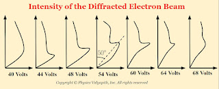
Working: When a low potential is applied to the electron gun so that a beam of slow electrons emerges from the gun and falls normally on the surface of the crystal. To collect the diffracted electrons, the Faraday cylinder is moved to various positions on the scale $S$ and the corresponding galvanometer measures the current at each position through an electron detector. The observation is repeated for electrons accelerated through different potentials. The current which is a measure of the intensity of the diffracted electron beam, is plotted against the diffracting angle $\phi$ for each accelerating potential as shown in the figure below
It is observed in the curves that at the voltage of $40$ volts, a smooth curve is obtained and a bump begins to appear in the curve for $44$ volts. As the potential difference is further increased, the bump starts shifting upward and becomes most prominent in the curve for $54$ volts at $\phi = 50 ^{\circ}$. Beyond $54$ volts the bump gradually diminishes and becomes insignificant at $68$ volts. The pronounced current peak at $54$ volts and at $50^{\circ}$ provided an evidence that electrons were diffracted by the target and verifies the existence of electron wave nature.
Calculation of Wavelength:
Theoretical Calculation:
The wavelength of electron at $54$ volts can be find by de- Broglie formula as shown in the equation $(3)$
$\lambda= \frac{12.28}{\sqrt{54}}\: A^{\circ}$
$\lambda= 1.671 \: A^{\circ} $
Experimental Calculation:
Experimental calculation is done by Bragg's diffraction equation
$n \lambda = 2d \: sin\theta$
Where
$d \rightarrow$ interplanar Spacing
$n \rightarrow$ Order of plane
For nickel crystal :
$n=1$
$d=0.91 A^{\circ}$
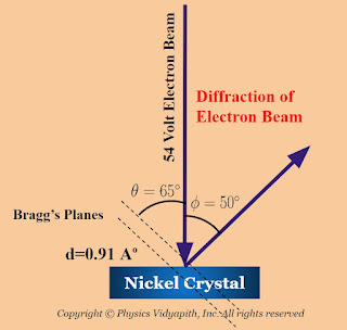
In the experiment, the diffracted electron beam appearing at $\phi=50 ^{\circ}$ aries from wave-like diffraction from the family of Bragg's planes.
The corresponding angle of incidence relative to the family of Bragg's planes is
$\theta = \frac{180 - \phi}{2}$
$\theta = \frac{180 - 50}{2}$
$\theta= 65^{\circ}$ Now apply these values to Bragg's equation as written above
$\lambda = 2 \times 0.91 \times sin 65^{\circ} $
$\lambda = 2 \times 0.91 \times 0.906 $
$\lambda = 1.65 A^{\circ} $
The theoretical and experimental value at $54$ volts verifies the wave nature of electrons by diffraction of the beam.
2. Target
3. Electron detector or Faraday's cylinder
4. Galvanometer 1. Electron gun: The electron gun is a device that is used to produce a highly accelerated and collimated electron beam by applying high potential.
$d \rightarrow$ interplanar Spacing
$n \rightarrow$ Order of plane
$n=1$
$d=0.91 A^{\circ}$
In the experiment, the diffracted electron beam appearing at $\phi=50 ^{\circ}$ aries from wave-like diffraction from the family of Bragg's planes.
The corresponding angle of incidence relative to the family of Bragg's planes is
$\theta = \frac{180 - \phi}{2}$
$\theta = \frac{180 - 50}{2}$
$\theta= 65^{\circ}$ Now apply these values to Bragg's equation as written above
Magnetic field at the center of circular loop
Mathematical Analysis of magnetic field at the center of circular loop:
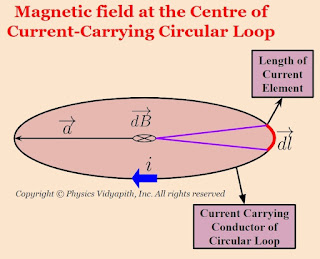
Let us consider, a current-carrying circular loop of radius $a$ in which $i$ current is flowing. Now take a small length of a current element $dl$ so magnetic field at the center of a circular loop due to the length of current element $dl$. According to Biot-Savart Law:
$dB=\frac{\mu_{\circ}}{4 \pi} \frac{i .dl .sin\: \theta}{a^{2}} $
Here $\theta$ is the angle between length of current element $\left( \overrightarrow{dl} \right)$ and radius $\left( \overrightarrow{a} \right)$. These are perpendicular to each other i.e. $\theta = 90^{\circ}$
$dB=\frac{\mu_{\circ}}{4 \pi} \frac{i .dl .sin\: 90^{\circ}}{a^{2}} $
$dB=\frac{\mu_{\circ}}{4 \pi} \frac{i .dl }{a^{2}} \qquad \left(1 \right)$
The magnetic field at the center due to a complete circular loop
$B=\int dB \qquad \left(2 \right)$
From equation $(1)$ and equation $(2)$
$B=\int \frac{\mu_{\circ}}{4 \pi} \frac{i .dl}{a^{2}}$
$B=\frac{\mu_{\circ}}{4 \pi} \frac{i}{a^{2}} \int dl $
For complete loop $\int dl = 2 \pi a$, So from above equation that can be written as
$B=\frac{\mu_{\circ}}{4 \pi} \frac{i}{a^{2}} \left( 2 \pi a \right) $
$B=\frac{\mu_{\circ} i}{2 a}$
This is an equation of the magnetic field at the center of the circular loop.
Ampere's Circuital Law and its Modification
Ampere's Circuital Law Statement:
When the current flows in any infinite long straight conductor then the line integration of the magnetic field around the current-carrying conductor is always equal to the $\mu_{0}$ times of the current.
$\int \overrightarrow{B}. \overrightarrow{dl} = \mu_{\circ} i$
Derivation of Ampere's Circuital Law:
Let us consider, An infinite long straight conductor in which $i$ current is flowing, then the magnetic field at distance $a$ around the straight current carrying conductor
$B=\frac{\mu_{\circ}}{2 \pi} \frac{i}{a}$
Now the line integral of the magnetic field $B$ in a closed loop is
$\oint \overrightarrow{B}. \overrightarrow{dl} = \oint \frac{\mu_{\circ}}{2 \pi} \frac{i}{a} dl$
$\oint \overrightarrow{B}. \overrightarrow{dl} = \frac{\mu_{\circ}}{2 \pi} \frac{i}{a} \oint dl$
$\oint \overrightarrow{B}. \overrightarrow{dl} = \frac{\mu_{\circ}}{2 \pi} \frac{i}{a} \left(2 \pi a \right) \qquad \left( \because \oint dl= 2 \pi a \right)$
$\oint \overrightarrow{B}. \overrightarrow{dl} = \mu_{\circ}i$
Modified Ampere's circuital law:
When the capacitor is placed in between the conductors then a current flows in the capacitor which is known as displacement current $\left(i_{d} \right)$. So modified Ampere's circuital law:
$\oint \overrightarrow{B}. \overrightarrow{dl} = \mu_{\circ} \left( i + i_{d} \right)$
Preparation of nanostructured particles by sol-gel method
Introduction:
The advent of the sol-gel process occurred in the year $1921$. In the $1960s$, its development was given due to the need for new synthesis methods in the nuclear industry.
The sol-gel method is a widely used wet chemical technique to fabricate nanostructured materials. This technique is used to prepare nanoparticles of ceramics, glassy, and composite materials at relatively low temperatures based on wet chemical processing. It involves the conversion of a precursor solution (i.e. sol) into a solid three-dimension network (i.e. gel) through hydrolysis and condensation reactions of precursor compounds. There are following steps are given below to fabricate nanostructured material through the sol-gel method.
1. Precursor Compound Selection:
The first step involves selecting the appropriate precursor compounds, usually metal alkoxides or inorganic salts, that will form the desired material upon hydrolysis and condensation. These precursors should be soluble in a solvent i.e. metal salt in water or metal alkoxide in an organic solvent like alcohol.
2. Hydrolysis (Formation of Sol):
It involves the conversion of a homogeneous solution of the precursor into a colloidal solution (i.e. The colloidal particles of precursor stably disperse in a solvent is called a Sol or colloidal solution.). In the hydrolysis process, Alcohol like ethanol or isopropanol is used as a solvent. Water or an acidic/basic catalyst is then introduced to initiate hydrolysis of the precursor molecules. This results in the breaking of metal-oxygen bonds in the precursor, generating metal hydroxide or oxide species. The reactions are given below.
$M-OR + H_{2}O \rightarrow M-OH +R-OH$
Where
$M=OR \rightarrow$ Metal Alkoxide
$M-OH \rightarrow$ Metal Hydroxide
$M \rightarrow Si, Ti,\: Zn,\: Al,\: Sn \:\: etc $
3. Condensation (Formation of Gel):
The colloidal solution is kept for aging. During aging, the various condensation chemical reaction (i.e. polymerization) between two metal hydroxyl species leads to $M-O-M$ bonds with the release of $h_{2}O / R-OH$. This condensation process continues till finally results in a gel interconnected, rigid, and porous inorganic networks covered completely with the liquid phase. This transformation is known as a sol-gel transition.
4. Gelation:
As the condensation reactions continue, the sol transforms into a three-dimensional network with a continuous solid phase interspersed with a liquid phase. This semi-solid network is known as a gel. The gelation process can be controlled by adjusting factors like precursor concentration, solvent composition, pH, and temperature.
5. Drying:
Once the gel has formed, the excess solvent is removed through a drying process. The drying can be done by various techniques such as evaporation, supercritical drying, or freeze-drying. Careful drying is essential to prevent cracking or collapse of the gel structure.
6. Xerogel:
If the solvent is dehydrated under ambient conditions (i.e. Removal of $R-OH$ groups). Xerogel is produced.
7. Calcination:
In many cases, the dried gel must undergo a thermal treatment called calcination. This involves heating the gel at elevated temperatures to remove any remaining organic components and to induce further crystallization and growth of the desired material. The final crystalline structure and properties of the nanostructured material are developed during this step.
8. Characterization:
The resulting nanostructured material is then characterized using various techniques like X-ray diffraction (XRD), scanning electron microscopy (SEM), transmission electron microscopy (TEM), and spectroscopy to analyze its composition, structure, particle size, and morphology.
Advantages of the Sol-gel process:
Versatile: Sol-gel method provides better control over the structure of particles, size of particles, and porosity. There is a possibility of incorporating nanoparticles and organic materials into sol-gel derived oxides.
Extended composition ranges: The sol-gel method allows the preparation of any oxide composition as well as also some non-oxides and the production of new hybrid organic-inorganic materials, which do not exist naturally.
Better Homogeneity: Due to mixing at the molecular level; high purity
Less energy consumption: There is no requirement for the melting temperature since the three-dimensional network structure can be achieved at relatively low temperatures.
Coating and thin films, monoliths, composites, porous membranes, powders, and fibers.
No need for special or expensive equipment.
Disadvantages of Sol-Gel:
Cost of precursors
Shrinkage of a wet gel upon drying, which often leads to fracture due to the generation of large capillary stresses and consequently, makes difficult the attainment of large monolithic pieces
Preferential precipitation of a particular oxide during the formation of colloidal solution i.e. Sol (in multicomponent glasses) due to the different reactivity of the alkoxide precursors
Difficult to avoid residual porosity and $OH$ groups.
Application of Sol-Gel:
Protective Coating
Thin films and fibers
Opto-mechanicalspan
Nanoscale powders
Medicine
$M-OH \rightarrow$ Metal Hydroxide
$M \rightarrow Si, Ti,\: Zn,\: Al,\: Sn \:\: etc $
$M-OR + HO=M \rightarrow M-O-M +R-OH$
Synthesis of Nanomaterials
In the field of nanomaterials, there are two main approaches to their synthesis and fabrication.
A.) Top-Down Approach
B.) Bottom-up Approach
These two approaches are based on the methods used to create or assemble nanoscale materials and structures.
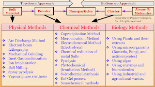
A.) Top-Down Approach: In this approach, large-scale materials (i.e. Bulk materials) are broken down into smaller and smaller components until they reach the desired nanoscale dimensions i.e. firstly the bulk material is converted into powder form and then the powder's form is converted into nanoparticles. There are various physical methods (like Arc discharge method, Electron beam lithography, Mechanical grinding, etc) used to convert the bulk material into powder form and powder form is converted into nanoparticles by chemical methods (like Sol-Gel Process, Electrochemical method, Microemulsion etc.).
One of the challenges with the top-down approach is that it may lead to a lack of control over the final nanomaterial's properties and may also generate waste during the process.
Top-down approaches are based on grinding the material. Thus these processes are subtractive in nature. The parts of mechanical devices used to shape the objects are stiff and hard, so these approaches are not suitable for soft samples. The top-down approach assumes that nanodevices must be produced piece by piece in a series of steps, much like manufactured goods are made. Scanning probe microscopy (SPM) is an important technique used both for the synthesis and characterization of nanomaterial by a top-down approach. Atomic force microscopy (AFM) tips can be used as a nanoscale "write head" to deposit a resist, which is then followed by an etching process to remove material in a top-down approach.
Some common techniques used in the top-down approach include:
a.) Mechanical milling: High-energy mechanical forces are applied to break down large particles into smaller ones, eventually reaching the nanoscale range.
b.) Lithography: Techniques like electron beam lithography or photolithography are used to create patterns on a substrate, defining the nanoscale features.
c.) Etching: Chemical or plasma etching is used to remove material from a larger sample, creating nanoscale structures.
d.) Nanolithography: Specialized lithography techniques are used to directly write or print nanoscale patterns on material.
Advantages of the Top-down Approaches:
1.) This Top-down approach is often suitable for large-scale production of nanomaterials, making it economically viable.
2.) Many top-down approaches have been widely used and optimized for bulk materials, which can be adapted for nanomaterial synthesis.
3.) This approach allows precise control over the size and shape of the resulting nanomaterials.
4.) Suitable for laboratory experimentation.
Disadvantages Top-down Approaches:
1.) It is required large installations and huge capital is required for building their setup.
2.) These approaches are quite expensive.
3.) The growth process is slow and hence these approaches are not suitable for large-scale production.
4.) The biggest problem in the approach is the imperfection of surface structure.
5.) The mechanical and chemical processes involved in the top-down approach can introduce defects in the nanomaterials, affecting their properties.
6.) This approach generates a significant amount of waste during the material reduction process, which can be environmentally problematic.
7.) As the approach starts with larger structures and reduces their size, it may be challenging to achieve precise control over nanoscale features, leading to variations in properties.
B.) Bottom-up Approaches: In this approach, It involves atom-by-atom, molecule-by-molecule, or cluster-by-cluster manipulation for the synthesis of nanostructures. It means that atoms are assembled into molecules, molecules are assembled into clusters, and the clusters are assembled to form the nanoparticle. This approach relies on self-assembly and controlled growth to create the desired nanoscale structure.
The bottom-up approach is based on the principle of molecular recognition (that is self-assembly). Self-assembly means growing more and more things of one's kind from themselves. The principle of self-assembly (shake and bake) involves assembling precursors in random positions and orientations, providing energy (shaking) to enable them to explore configuration space. The hugeness of this space suggests that a convergent pathway is inherent in the process in order to allow it to be completed in a reasonable time. Once the precursors are in position, "baking" may be required to strengthen the bonds connecting them and fix the final object permanently.
Some common techniques used in the bottom-up approach include:
a.) Chemical Synthesis: Chemical reactions are used to build up nanomaterials from atomic or molecular precursors, allowing precise control over the final product's size and shape.
b.) Self-Assembly: Molecules or nanoparticles are designed to interact in a way that leads to their spontaneous arrangement into specific nanoscale structures.
c.) Vapor Deposition: Nanoscale materials are grown layer by layer on a substrate by allowing precursor gases to react on its surface.
d.) Sol-Gel Process: Nanomaterials are formed by hydrolyzing metal alkoxides in a solution, followed by gelation and controlled drying.
The bottom-up approach allows for greater control over the nanomaterial's properties and can potentially lead to unique properties not found in their bulk counterparts. However, it can be more challenging to scale up these processes for mass production compared to the top-down approach.
Advantages of Bottom-down Approaches:
1.) The bottom-up approach allows for precise control at the atomic or molecular level, leading to well-defined nanomaterials with specific properties.
2.) Since the materials are assembled from individual atoms or molecules, there are fewer defects compared to the top-down approach.
3.) Bottom-up synthesis can result in unique nanomaterials with properties not easily achievable through top-down approaches.
Disadvantages of Bottom-down Approaches:
1.) Bottom-up approaches can be more complex and expensive, especially for large-scale production.
2.) Some bottom-up approaches may not be easily scalable for mass production, limiting their industrial applicability.
3.) Achieving high purity and reproducibility in bottom-up synthesis can be challenging due to the intricate processes involved.
Both the top-down and bottom-up approaches have their advantages and disadvantages, and researchers often choose the most suitable method based on the specific properties and applications of the nanomaterial they aim to create. Additionally, a combination of these approaches, known as "hybrid approaches," can be used to achieve even more complex nanoscale structures with tailored properties.
The synthesis of nanomaterial according to technique:
1.) Physical Methods
2.) Chemical Methods
3.) Biological Methods
1.) Physical Methods: Nanoparticles may be synthesized using a number of physical methods which are listed below. These methods are of two types viz mechanical type and vapor deposition type. These methods work at very high temperatures. The highest working temperatures are usually greater than $350^{\circ}C$.
- Arc Discharge Method
- Electron beam Lithography
- Mechanical Grinding
- Inert Gas condensation
- Ion Implantation
- Ball Milling
- Spray pyrolysis
- Vapour phase synthesis
- Coprecipitation Method
- Microemulsion Method
- Electrochemical Method (Electrolysis)
- Chemical reduction of metal Salts Pyrolysis
- Phytochemical (irradiation Method)
- Solvothermal synthesis
- Sol-Gel process
- Sonochemical methods
- Using Plants and their extracts
- Using microorganisms (Bacteria, Fungi, and actinomycetes)
- Using algae
- Using enzymes and biomolecules
- Using industrial and agricultural wastes
Basics and types of Nanomaterials
What is a nanoparticle?
Those particles that have size ranges between $1$ to $100 \: nanometres$ are called a nanoparticle. The particles are undetectable by the human eye. There are significant differences in the properties (like magnetic, electrical, Structural, Mechanical, and optical properties) of nanoparticles and bulk materials.
What is nanomaterial?
Those materials that have at least one dimension should be in nanometres i.e. $10^{-9}m$ are called nanomaterials. The prefix 'nano' means a billionth $(10^{-9})$.
Types of nanomaterials
There are two types of nanomaterial that can be classified:
A.) On the basis of dimension
B.) On the basis of material
A.) On the basis of dimensions: According to Siegel, nanostructured materials are classified on the basis of dimension:
1.) Three-dimensional nanomaterials (Bulk Nanomaterial)
2.) Two-dimensional nanomaterials (Quantum Well)
3.) One-dimensional nanomaterials (Quantum Wire)
4.) Zero-dimensional nanomaterials (Quantum Dot)
1.) Three-dimensional nanomaterials (Bulk Nanomaterial): These nanomaterials have not confined to the nanoscale range in any dimension. These materials have three arbitrary dimensions above the nanoscale i.e. $100 nm$. The bulk three-dimensional nanomaterials are composed of a multiple arrangement of nano-size crystals in different orientations. The three-dimensional nanomaterials or bulk nanomaterials can be used as bundles of nanowires, dispersion of nanoparticles, and nanotubes as well as multi-nano layers (polycrystals) in which the $0D$, $1D$, and $2D$ structural elements are in very close contact with each other and form interfaces.
2.) Two-dimensional nanomaterials (Quantum Well): These nanomaterials have one dimension in the nanoscale. It is also called a quantum well. This means that the particles of material are confined only along one dimension. The 2D nanomaterials exhibit plate-like shapes. It includes nanofilms, nanolayers, and nanocoatings with nanometre thickness.
3.) One-dimensional nanomaterials (Quantum Wire): These nanomaterials have two dimensions in the nanoscale. It is also called quantum wire. This means that the particles of material are confined in two dimensions. This leads to needle-shaped nanomaterials. It includes nanofibers, nanotubes, Nanorods, and nanowires.
4.) Zero-dimensional nanomaterials (Quantum Dot): These nanomaterials have all three dimensions in the nanoscale i.e., no dimensions are greater than $100 nm$. It is also called quantum dots. This means that the particles of material are confined in all three dimensions. It includes Nanospheres and nanoclusters.
B.) On the basis of materials: Nanomaterials can be categorized on the basis of material into four types such as:
1.) Inorganic-based nanomaterials (Metal-based materials ):
2.) Carbon-based nanomaterials:
3.) Organic-based nanomaterials (Dendrimers):
4.) Composite-based nanomaterials.
1.) Inorganic-based nanomaterials (Metal-based materials ):
Generally, inorganic-based nanomaterials include different metal and metal oxide nanomaterials.
Examples of metal-based inorganic nanomaterials - silver $(Ag)$, gold $(Au)$, aluminum $(Al)$, cadmium $(Cd)$, copper $(Cu)$, iron $(Fe)$, zinc $(Zn)$, and lead $(Pb)$ nanomaterials.
Examples of metal oxide-based inorganic nanomaterials- zinc oxide $(ZnO)$, copper oxide $(CuO)$, magnesium aluminum oxide $(MgAl_{2}O_{4})$, titanium dioxide $(TiO_{2})$, cerium oxide $(CeO_{2})$, iron oxide $(Fe_{2}O_{3})$, silica $(SiO_{2})$, and iron oxide $(Fe_{3}O_{4})$, etc.
(2) Carbon-based nanomaterials:
Carbon-based nanomaterials are graphene, fullerene, single-walled carbon nanotube, multi-walled carbon nanotube, carbon fiber, activated carbon, and carbon black.
(3) Organic-based nanomaterials (Dendrimers):
The organic-based nanomaterials or dendrimers (i.e. Dendrimers are repetitively branched molecules. Dendrimers name comes from the Greek word ‘dendron’ which means tree.) are formed from organic materials that do not include carbon materials, for instance, dendrimers, cyclodextrin, liposome, and micelle.
(4) Composite-based nanomaterials: The composite nanomaterials can be any combination of all nanomaterials like metal-based, carbon-based, metal oxide-based, and organic-based nanomaterials. These composite nanomaterials have very complicated structures like a metal-organic framework.
Electric field intensity due to thick hollow non-conducting sphere
Electric field intensity at different points in the field due to uniformly charged thick hollow non-conducting sphere:
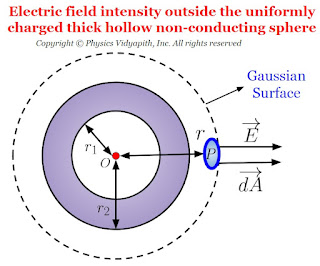
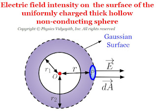
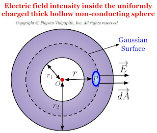
Let us consider, A hollow non-conducting sphere of inner radius $r_{1}$ and outer radius $r_{2}$ in which $+q$ charge is evenly distributed evenly in the entire volume of the sphere. If $\rho$ is the volume charge density then electric field intensity at different points on the electric field of the thick hollow non-conducting sphere:
- Electric field intensity outside the thick hollow non-conducting sphere
- Electric field intensity on the surface of the thick hollow non-conducting sphere
- Electric field intensity at an internal point of the non-thick hollow conducting sphere
Characteristics of Electromagnetic Wave
Electromagnetic Wave:
An electromagnetic wave is the combined effect of an electric field and magnetic field which carry energy from one place to another.
When an electric field and the magnetic field are applied perpendicular to each other then a wave propagates perpendicular to both the electric field and the magnetic field. This wave is called the electromagnetic wave.
Characteristics of Electromagnetic Wave:
1.) Electric and Magnetic Fields: Electromagnetic waves are produced through the mutually perpendicular interaction of electric and magnetic fields. The propagation of the wave is also perpendicular to both the electric field and the magnetic field.
2.) Wave Nature of electromagnetic waves: Electromagnetic waves are characterized by their wave-like behavior, so they exhibit the properties such as wavelength, frequency, amplitude, and velocity. This wave-like behavior of electromagnetic waves can undergo phenomena like interference, diffraction, and polarization.
3.) The spectrum of an electromagnetic wave: In the spectrum of electromagnetic waves, All the wavelengths and frequencies of the waves are included such as radio waves, microwaves, infrared, visible light, ultraviolet, X-rays, and gamma rays etc.
4.) Speed of electromagnetic wave: The speed of electromagnetic waves in free space or vacuum is equal to the speed of light in free space or vacuum, which is approximately 299,792 $Km/s$.
5.) Transverse waves of an electromagnetic wave: Electromagnetic waves are transverse waves which mean that the oscillations of the electric and magnetic fields occur perpendicular to the direction of wave propagation.
6.) Dual nature of electromagnetic wave: Electromagnetic waves have both wave-like and particle-like behavior. They can be described as a stream of particles called photons, each photon carrying a specific amount of energy (quantum). This duality is described by the wave-particle duality principle in quantum mechanics.
7.) Energy transfer in electromagnetic waves: Electromagnetic waves transport energy through space. The amount of energy carried by each wave depends on its frequency. Higher frequency waves, such as gamma rays and X-rays, carry more energy than lower frequency waves like radio waves.
8.) Absorption, Reflection, and Transmission of Electromagnetic waves: Electromagnetic waves can be absorbed by certain materials, reflected off surfaces, or transmitted through transparent substances. The behavior of waves at boundaries depends on factors such as the angle of incidence, the nature of the material, and the frequency of the wave.
9.) Electromagnetic Induction of electromagnetic wave: When electromagnetic waves interact with conductive materials or circuits, they can induce electric currents or voltages. This principle is the basis for technologies like antennas, wireless communication, and electromagnetic sensors.
10.) Electromagnetic Interactions of electromagnetic waves: Electromagnetic waves can interact with matter in various ways, including absorption, scattering, and emission. These interactions are utilized in fields such as optics, spectroscopy, medical imaging, and telecommunications.
Popular Posts
-
Let $S$ be a point monochromatic source of light of wavelength $\lambda$ placed at the focus of collimating lens $L_{1}$. The light beam is ...
-
Angle of Acceptance → "If incident angle of light on the core for which the incident angle on the core-cladding interface equals t...
-
Derivation of interference of light due to a wedge-shaped thin film: Interference of light due to wedge-shaped thin film The wedge...
-
Maxwell's Equations: Maxwell's equation of the electromagnetic wave is a collection of four equations i.e. Gauss's law of elec...
-
Let a plane wavefront be incident normally on slit $S_{1}$ and $S_{2}$ of equal $e$ and separated by an opaque distance $d$.The diffracted l...
Study-Material
Categories
Alternating Current Circuits
(10)
Atomic and Molecular Physics
(4)
Biomedical
(1)
Capacitors
(6)
Classical Mechanics
(12)
Current carrying loop in magnetic field
(5)
Current Electricity
(10)
Dielectric Materials
(1)
Electromagnetic Induction
(3)
Electromagnetic Wave Theory
(23)
Electrostatic
(22)
Energy Science and Engineering
(2)
Error and Measurement
(2)
Gravitation
(11)
Heat and Thermodynamics
(3)
Kinematics Theory Of Gases
(2)
Laser System & Application
(15)
Magnetic Effect of Current
(9)
Magnetic Substances
(3)
Mechanical Properties of Fluids
(4)
Nanoscience & Nanotechnology
(4)
Nuclear Physics
(7)
Numerical Problems and Solutions
(2)
Optical Fibre
(5)
Optics
(25)
Photoelectric Effect
(3)
Quantum Mechanics
(34)
Relativity
(8)
Semiconductors
(2)
Superconductors
(1)
Topic wise MCQ
(9)
Units and Dimensions
(1)
Waves
(5)






.jpg)
.jpg)
.jpg)
.jpg)
